What is FPGA?
So, what is FPGA? According to Wikipedia, “a field-programmable gate array (FPGA) is an integrated circuit designed to be configured by the customer or designer after manufacturing—hence “field-programmable”.”.
The FPGA contains a whole lot of logic gates that can be configurable by customers in any way they like. It means that we can create our own integrated circuit on this chip. We can do a simple multiplexer from it and make a memory controller, microcontroller or CPU. We can even put the whole computer inside it! Amazing!
The main FPGA characteristic is the number of logic gates that it has. For instance, the most basic Altera Cyclone chip has about 5,000 gates. It’s a lot! For example, a CPU like Z80 or 6502 requires 1,000 to 2,000 gates. The retro computer based on those CPUs will take 3,000 – 6,000 gates. Apart from the gates, FPGA typically has some memory (not much, usually around 50-100 kilobytes) and several PLLs.

FPGAs are not expensive as well. A decent chip for most hobby projects costs $10-$20.
A special language is used to program FPGA. The most popular ones are VHDL and Verilog. Each of them has its benefits. They can be mixed into one project, so it is good to know both of them.
I prefer VHDL because I find that it gives better control. But some tasks are easier to do in Verilog.
Those languages are not program languages like C or BASIC. They are used to describe the schematic. The typical project consists of “processes”. Each process does its job independently from the others. Processes communicate with each other by “signals”, just like typical electronic components do. Usually, all operations are synchronised by clock signals.
FPGA design should have the same considerations as in usual digital electronic design. For instance, signal timing should be considered to avoid “signal racing”, as in traditional design. Even basic FPGAs are good enough to use 50MHz or even 100MHz clocks. More than enough for any retro computer!
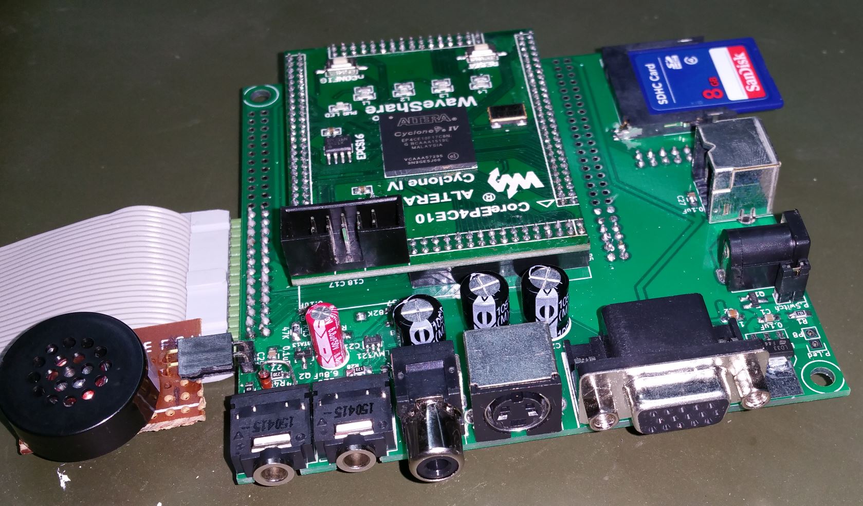
To create and debug devices on FPGA, it is essential to have a good development board with a chip that will be used in a project. There are several manufacturers of FPGAs, but the most popular are Altera and Xilinx. I use Altera for my projects because I have an Altera development board. The main principles are the same, so it is relatively easy to switch between those brands.
There is a free version of the software called “Quartus” to program Altera devices. It can be downloaded from the Altera site. I use a Terasic DE1 development board with an Altera Cyclone II chip.

This board is almost perfect for hobby projects. Check it out:
- Altera Cyclone II 2C20 FPGA with 20,000 LEs (more than enough for hobby projects)
- USB Blaster built in on board for programming and user API controlling (don’t need a programmer)
- 8Mbyte (1M x 4 x 16) SDRAM, 4Mbyte Flash Memory, 512Kbyte (256K x 16) SRAM (decent amount of memory for most projects)
- SD Card Socket
- 4 Push-button switches and 10 DPDT switches
- 8 Green User LEDs, 10 Red User LEDs, and 4 Seven-segment LED displays (great for debugging)
- 50MHz oscillator, 24MHz oscillator, 27MHz oscillator and external clock sources
- 24-bit CD-Quality Audio CODEC with line-in, line-out, and microphone-in jacks
- VGA DAC (4-bit R-2R per channel) with VGA out connector
- RS-232 Transceiver and 9-pin connector
- PS/2 mouse/keyboard connector
- Two 40-pin Expansion Headers (in case you want to connect something else)
This board costs $150 plus delivery from the Terasic site.
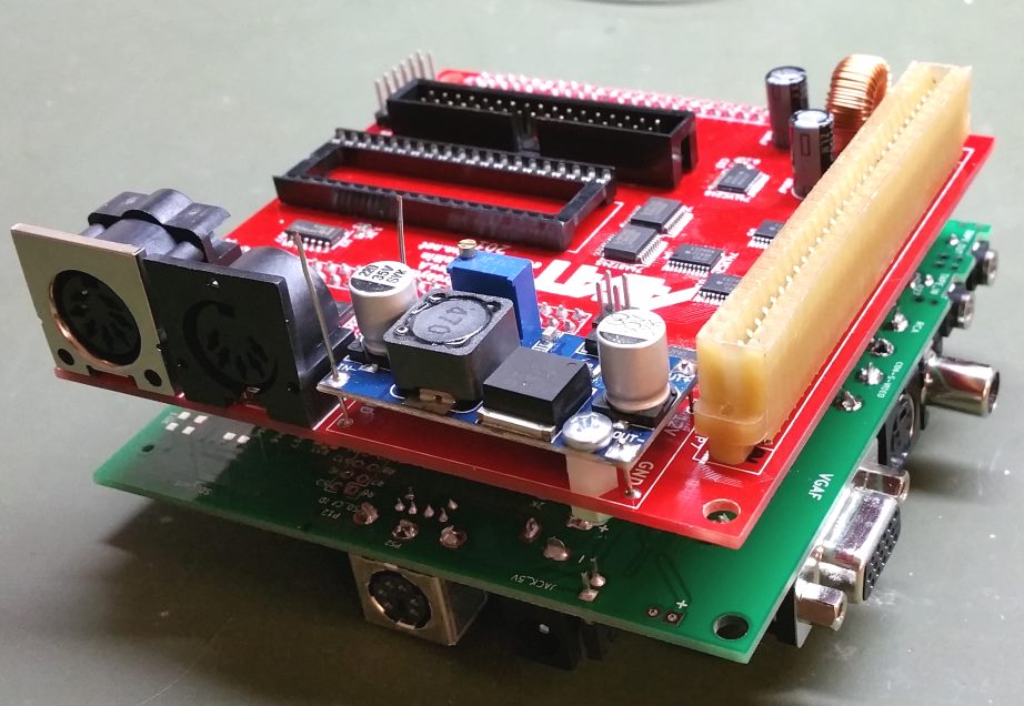
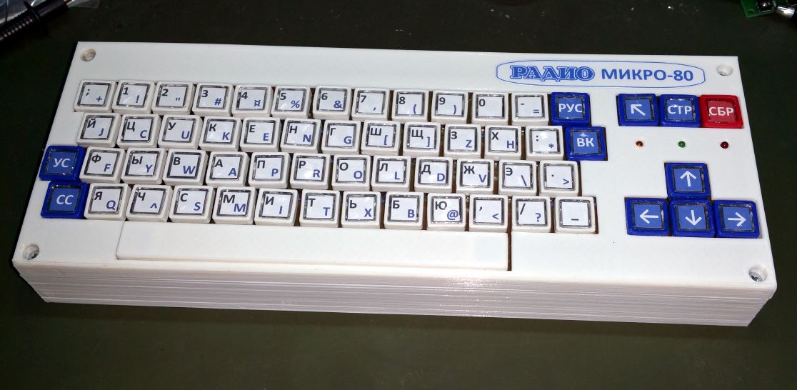
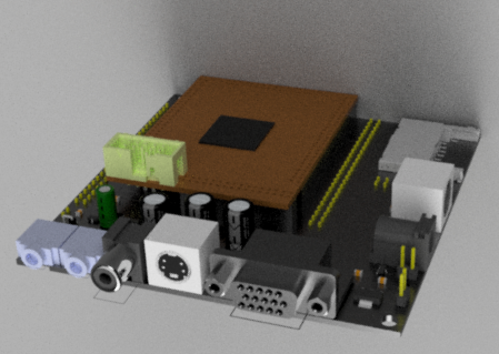
I will use this board to make a replica of the “UT-88” computer I briefly described in the previous post. Let’s see how it goes.