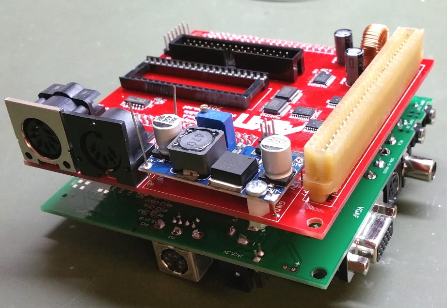
Retrobyte Rev.B
In my previous post, I explained my idea of a modular platform for building modern replicas of retro-computers, of which the Rev.A has already been built and tested. In the process, I found a few things to improve:
- On the silkscreen, the diode D1 was shown incorrectly (the cathode points to the anode)
- The signal’s voltage from the speaker input, which leads to the FPGA, was too high (4.2V). To lower it to 3.2V, a R46 27K resistor was added
- The labels PAL and NTSC near the resistors R11 and R12 have been mixed up
- The places to solder the U2, U3 and IC1 chips to the board are too short to comfortably hand-solder. They need to be extended.
- The first pin of the IC1 chip is not labelled.
- In the schematic, the numbers of the pins connected to SDRAM were mixed up. This mistake was easily fixed in the firmware of the FPGA, yet this still needed to be adjusted on the schematic.
- Some incorrectly labelled pins (J7 needs to be F7 and F7 needs to be E7). Yet again, this can be fixed using the FPGA firmware, but some changes were still applied to the circuit and silkscreen.
As you can see here, the improvements are mostly cosmetic (except #2)
Here are the updated schematics, Rev.B:
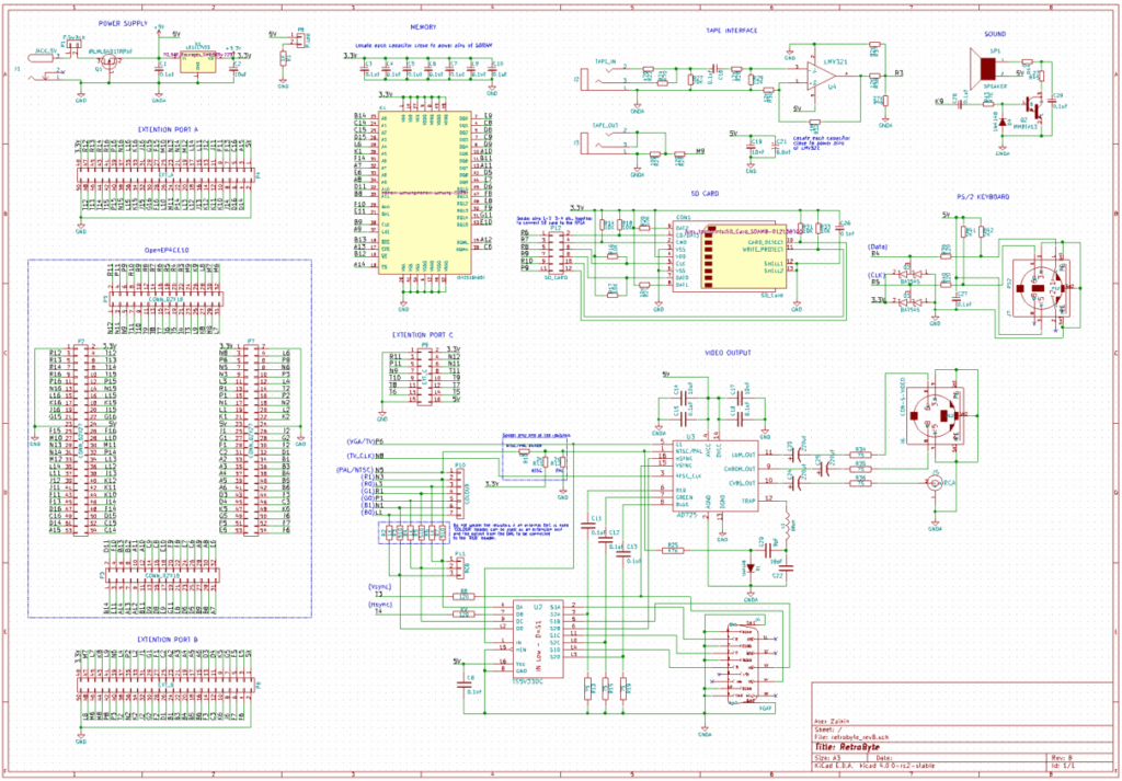
You also can download the BOM and Gerber files. In the BOM, the resistors and capacitors are type 0805 if not specified. Also, I provided some component codes for element14, RSOnline and DigiKey for reference.
WARNING! This revision was not yet tested, so there will likely be some mistakes in the schematics, board or BOM. If you choose to replicate the schematic, please be careful and check everything yourselves; also note that you are doing this at your own risk, and any complaints will not be welcome. Retrobyte is still a work in progress, and of course, I will be grateful for any comments on any inaccuracies or mistakes I have made.