Agat-7. Rev.0. Video output.
I’ve spent some time debugging STM32L based 140K “floppy drive” for my “Agat-7” replica project. It is already perfectly workable in read-only mode. I transferred it to the SPI interface to save some FPGA pins, and now I need only five pins instead of 12. For an 840K floppy drive, it will save even more pins. But the wires and cables that I used for connections created a lot of errors in the SPI protocol, so I had to send each byte by three times. If the transfer were reliable, I wouldn’t need the 5th pin, so I can potentially reduce the required wires to 4 later on PCB. Here is the quality of the SCLK signal after reaching the STM32L development board from DE1:

As you can see, the capacitance is too high.
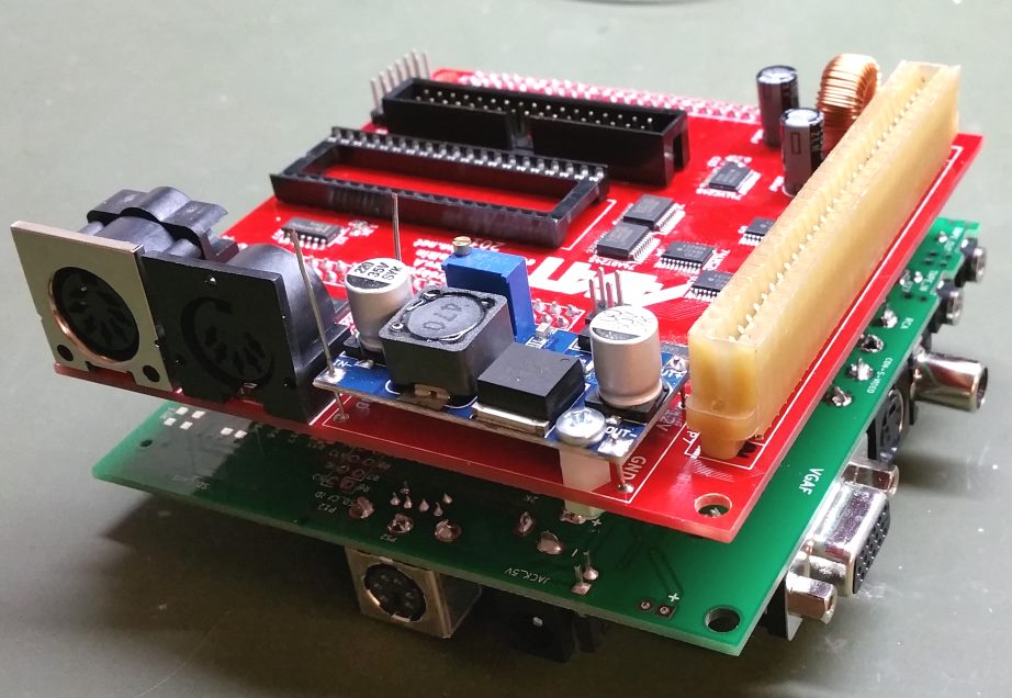
Having such a problem, it is difficult to continue the project, so I’ve created a Rev.0 PCB of the computer. It will also help me to debug other parts, like the I2C port extender or video output.
I’ve started to create a schematic of the replica. Compared to the final version, this revision won’t be made to fit any particular case; it will have some test pins for easier debugging, it won’t have a serial-parallel interface built in, and it won’t have an extension slot for original cards. But all unused FPGA pins will be accessible through the IO port, so it will be possible to add and debug the rest futures.
So, today I’m presenting the video output module. It allows using a VGA display with a resolution 1024х768х65Hz or a PAL-compatible TV set with a composite or S-Video input. Here it is:

The “SW_VGA” switch is used to choose output. It also connects to FPGA through an I2C port extender to switch the output standard.
Video output requires six pins of the FPGA: Red, Green, Blue, Y, HSync and VSync. They come from FPGA in the required format. Luminance (Y) bit is standard for all colours, but we must combine it with each colour signal separately. A simple 2-bit DAC on resistors is used for this purpose, but we need to ensure that the Y signal is mixed with a colour signal only if the colour signal is on. I used 74ALVC08 (U6) for this. It is a speed version of the popular AND-gates set 74HC08. It is essential to use this IC because its propaganda delay is less than 3ns which is more than ten times less than the smallest displayed pixel in the most condensed ANM-64 mode of the replica. The standard 74HC08 will have a delay of about 12ns, which is too high. Also, the benefit of this chip is its 3.3V voltage.
All colour signals are terminated by 75ohm resistors in the monitor or near PAL coder chip AD725 used in the project, so resistors R7-R12 effectively create a voltage divider with them. They have been chosen so the final voltage does not exceed standard 0.714V, and dots with lower luminance are readable.
After that, the colour signals go to an analogue switch TS5V330C, which directs them to the VGA monitor or TV output circuit, depending on the “SW_VGA” switch.
TV signal is coded with AD725 coder. Its recommended layout is described pretty well in the datasheet. I want to mention that it receives its clock signal from a generator on 17.734475MHz crystal and 74HC04 invertor. I haven’t used FPGA for this because both PLLs are used in the project already. Also, it saves another pin of the FPGA.
Sync signals HSYNC and VSYNC can be connected straight to both outputs because they are not terminated. I’ve connected the “VGA_VSYNC” signal this way. But because I have a spare (fourth) switch in TS5V330C IC anyway, I’ve connected “VGA_HSYNC” through it.
I would appreciate it if you find any mistakes in the schematic or have ideas to improve it. I’m going to create a PCB layout next week. I’ll publish the other parts of the schematic here as soon as they finish. See you!